
| Problem 1 (a), EE 4720 1997 Practice Midterm Exam Solution | Top Next |
First, we need to determine how addbi will execute.
The pipeline execution diagram below shows the progress of addbi
through the pipeline. The big immediate is shown on a second line, note
that it trails the "main" part of the instruction by one cycle.
Time:    0  1  2  3  4  5
addbi    IF ID EX ME WB
big im      IF ID EX ME WB
One possible solution uses a 3-input ALU so that all three operands can be added together at once. Since the big immediate is one cycle behind the other two operands they will have to wait in EX during cycle 2. The big immediate arrives in cycle 3, and they are all added together.
In a much better solution the two register operands would be added in cycle 2 and their sum would be added to the big immediate in cycle 3. There are two advantages to this scheme: a three-operand ALU is not needed (the two-operand ALU can be used as is) and there is no need to provide special storage or bypass paths for the two operands that would have had to return to EX in cycle 3.
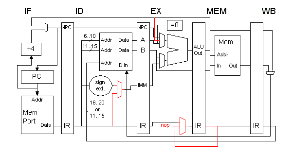
The pipeline changes are shown below in red, these also include control path modifications. Here the bypass path from MEM to EX was added, but nothing would have to be added to pipelines that already contained the bypass paths needed to avoid RAW hazards.
| Problem 1 (b), EE 4720 1997 Practice Midterm Exam Solution | Top Previous Next |
There is a dependency between lw
and addbi, and so addbi must stall in ID.
Note that addbi is two words; the diagram below shows
these as though they were separate instructions, but addbi2
is just the 32-bit immediate. Instruction addbi does
its register write in cycle 7, the WB at cycle 6 has no effect.
Time:  0  1  2  3  4  5  6  7
lw    IF ID EX ME WB
addbi    IF ID -> EX ME WB
addbi2      IF -> ID EX ME WB
sub               IF ID EX ME WB
| Problem 2 (a), EE 4720 1997 Practice Midterm Exam Solution | Top Previous Next |
Average CPI will be computed by taking a weighted average of instruction execution time, partitioned into these categories:
If all branches are predicted taken:
CPI = 0.1( 0.7 * 3 + 0.3 * 2 ) + 0.05 * 3 + 0.85 * 1Note that the CPI contribution of an instruction that stalls s cycles is s+1. If all branches are predicted not taken:
CPI = 0.1( 0.7 * 5 + 0.3 * 1 ) + 0.05 * 3 + 0.85 * 1| Problem 2 (b), EE 4720 1997 Practice Midterm Exam Solution | Top Previous Next |
With perfect branch prediction all taken branches stall 3 cycles and all not-taken branches stall 1 cycle:
CPI = 0.1( 0.7 * 3 + 0.3 * 1 ) + 0.05 * 3 + 0.85 * 1Not that much better than predicting all branches will be taken, especially considering that prediction was perfect.
| Problem 2 (c), EE 4720 1997 Practice Midterm Exam Solution | Top Previous Next |
So what if prediction isn't perfect, but right 80% of the time? In this case we need to enumerate additional cases:
CPI = 0.1( 0.7 ( 0.8 * 3 + 0.2 * 5 ) + 0.3 * (0.8 * 1 + 0.2 * 2 )) + 0.05 * 3 + 0.85 * 1It looks like just predicting all branches taken works better.
| Problem 3 (a), EE 4720 1997 Practice Midterm Exam Solution | Top Previous Next |
For each field that specifies a register, add a register size field. For example, consider a system using 10-bit opcodes:
| Field | Size | Comment |
| OP | 10 | Opcode field. (Size assumed.) |
| rd | 5 | Destination register number. |
| rds | 8 | Destination data size. |
| rs1 | 5 | Source register number. |
| rs1s | 8 | Source register size. |
| rs2 | 5 | Source register number. |
| rs2s | 8 | Source register size. |
| Problem 3 (b), EE 4720 1997 Practice Midterm Exam Solution | Top Previous Next |
In such a system registers could be identified by two numbers, an offset and a size. The offset would indicate where in the 2048-bit register memory the data would start, and the size would indicate its extent. A possible format would be:
| Field | Size | Comment |
| OP | 10 | Opcode field. (Size assumed.) |
| rd | 11 | Destination register offset. |
| rds | 8 | Destination register size. |
| rs1 | 11 | Source register offset. |
| rs1s | 8 | Source register size. |
| rs2 | 11 | Source register offset. |
| rs2s | 8 | Source register size. |
Note: such a register scheme is highly impractical because
of the number of bits needed to code operands, the flexibility
required of the register file, and the difficulty of determining
if two "registers" overlap.
| Problem 4 (a), EE 4720 1997 Practice Midterm Exam Solution | Top Previous Next |
Twenty bits would be needed for each operand field (in instructions), which would make the instruction size cumbersome.
Unless interrupt handlers had some way of knowing which registers were being used, all of them would have to be saved and restored each time a handler was run (which is often). The stack frame would also be quite large.
| Problem 4 (b), EE 4720 1997 Practice Midterm Exam Solution | Top Previous Next |
Consider a pipeline with bypass paths so the r2 value written by add can be bypassed to lw, avoiding a stall.
Time             0  1  2  3  4  5
add r2, r3, r4   IF ID EX ME WB
lw r1,(r2)+	    IF ID EX ME WB
Without special precautions, r2 will have its correct value at the end of cycle 3 (since it's written in the EX stage by lw). At cycle 4, that correct value will be overwritten by the add instruction: an incorrect execution due to a WAW hazard.


| David M. Koppelman - koppel@ee.lsu.edu | Modified 11 Mar 1998 20:08 (2:08 UTC) |