|
|
RF MEMS switch with in-plane, bistable, electromagnetic actuators for high power applications
Conventional RF MEMS switches for a millimeter wave frequency range have a capacitive-shunt type configuration with high voltage operated, out-of-plane electrostatic actuators [1]. Figure 1 shows the schematic diagram of the proposed RF MEMS switch that exploits in-plane, bistable, electromagnetic actuators.
- From an RF circuit point of view, it is similar to a typical coplanar waveguide except that its ground lines are floated. Hence, as fabricated, the switch is at on-state (figure 1a).
- When current flows as depicted in figure 1b, the actuators are snapped towards the ground lines pushing them to make contacts with a signal line. Due to huge impedance mismatch, most of the RF signal is reflected back to the input, thus this is called an off-state.
- To secure contacts between the ground lines and the signal line at this state after current withdrawal, the switch has to be designed so that restoring force of the ground line is smaller than that of the actuator at this displacement.
- When current flows as indicated in figure 1a, the actuators are snapped to their original positions, sending the switch back to the on-state again.
- To prevent short between the signal line and the ground lines, and between the ground lines and the actuators, dielectric material has to be coated on sidewalls.
- Not to add another lithography step, this dielectric can be deposited conformally, and then etched anisotropically so that it is only remained on the sidewalls. Parylene C is one of good candidates for this purpose.
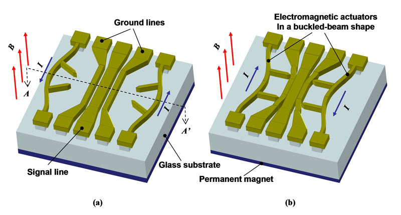 Fig. 1. Schematic diagram of the RF MEMS switch at (a) on-state and (b) off-state.
- The switch has following characteristics.
- The switch consumes no standing power due to bistability of the actuators.
- The switch operates at very low voltage, e.g. < 1 V.
- Since the actuators do not face the signal line, they are less susceptible to high power RF signal.
- Dielectric charging problem, one of the major failure problems of the conventional capacitive-type MEMS switches, is not severe in the proposed switch because it is operated at low voltage, and also voltages on the actuators keep changing their polarities.
- Parasitic inductance of the actuators does not affect the switch performance because the actuators are not part of an RF circuit.
- Fabrication process is much simpler than that of the conventional devices. Moreover, entire process can be completed using just a single mask, which means that it does not require an expensive mask aligner.
- Figure 2 shows the fabrication process flow of the switch device.
- It is fabricated on a Borofloat glass wafer which is not only a good dielectric substrate for RF passive devices (tan δ = 0.004) but also an attractive MEMS sacrificial substrate for its fast etch rate in concentrated HF (6-7 μm/min).
- First, Cr/Cu is evaporated as a seed layer.
- Then, photolithography is performed with thick SU-8 resist as electroplating molds (figure 2a).
- Next, copper is electroplated as a structural material (figure 2b).
- Then, SU-8 resist is stripped and seed metal is etched (figure 2c).
- Next, parylene is conformally coated (figure 2d), and then anisotropically etched without patterning so that it remains only on the sidewalls (figure 2e).
- Finally, the device is released by etching of the glass substrate in HF (figure 2f).
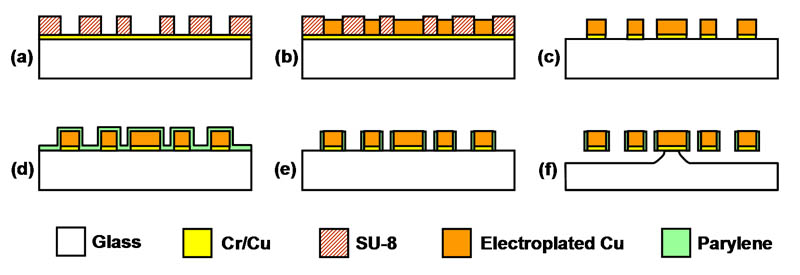 Fig. 2. Fabrication process flow of the RF MEMS switch.
*Ref. 1. JZ Yao, et al, "Micromachined low-loss microwave switches," IEEE J. MEMS, 8, 129-34, 1999.
|
