## LSU EE
3755 -- -- Computer Organization
#
## Control
Logic for MIPS -- fall 2006
##
Contents
#
# Single Cycle control
logic for the Datapath (page 85)
# Hard wired and Micro
Programmed Controller
# Multi Cycle control
logic
# Finite State Diagram
and Finite State Machine
# Programmable Logic
Array
# Single Cycle control
logic for the Datapath (page 85)
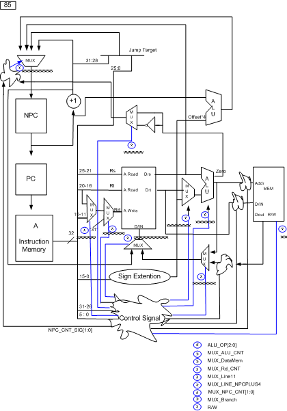
Control logic for Page 85 of
Datapath..
We simply have to give a control signal for each
Multiplexor , the ALU
and design logic for control circuit near the PC.
1) the ALU
2) Mux at ALU
3)Mux at
data Memory and ALU.
4)Mux at Rd for
Register file
5)Mux at line 15-11 for Register
file
6)Mux at D/IN for Register
file
7) Mux and control for NPC
8)Mux for the control after the
ALU
1) the ALU
ALU can
perform
AND,
OR,
SLT,
ADD,
SUB
operations.
We will generate
those control signals from
OP code
field[31:26] and func field[5:0]
We
have control inputs for ALU.
ALU_OP[2:0]
Operation
000
AND
001
OR
010
SLT
011
ADD
100
SUB
OP
FUN
ALUoperation : OP
FUN
ALU_OP
AND
0
0X 24
AND
000000 100100
000
ANDI
6
X
AND
000110 XXXXXX
000
OR
0
0x25
OR
000000 100101
001
ORI
d
X
OR
001101 XXXXXX
001
SLT
0
0x2a
SLT
000000 101010
010
SLTI
a
X
SLT
001010 XXXXXX
010
ADD
0
0X20
ADD
000000 100000
011
ADDI
8
X
ADD
001000 XXXXXX
011
SUB
0
0X22
SUB
000000
100010
100
LW
23
X
ADD
100011 XXXXXX
011
LB
20
X
ADD
100000 XXXXXX
011
SW
2b
X
ADD
100000 XXXXXX
011
SB
28
X
ADD
101000 XXXXXX
011
BEQ
4
X
SUB
000100 XXXXXX
100
BNE
5
X
SUB
000101 XXXXXX
100
By using AND and OR gates,
We could easily generate ALU_OP.
After logic minimization, the output will be
simpler.
##############################################################
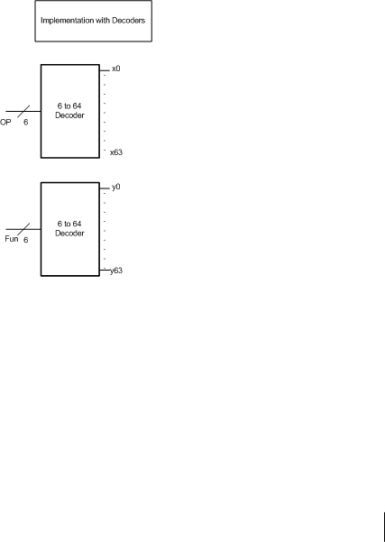
There are many other ways to do this.
One simple way is using decoders to decode OP code and function
field.
6 inputs and 64 outputs for each decoder.
000
AND
001
OR
010
SLT
011
ADD
100
SUB
ALU_OP[2] = x0 y34 +
x4 + x5
ALU_OP[1] = slt add (0 2a) + a + (0 20) + 8 + 23 + 20 +2b + 28
=
x0y42+x10+x0y32+x8+x35+x32+x43+x40
ALU_OP[0] = or add (0 25) + d+ (0 20) + 8 + 23 + 20 +2b + 28
= x0y37+x13+
x0y32+x8+x35+x32+x43+x40
##
Fig. for Decoders
###################################################################
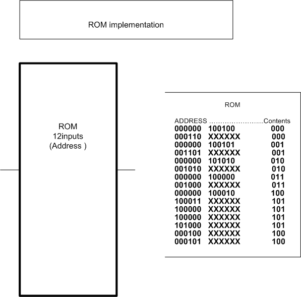
second simple way is using a ROM.
the address for the ROM is OP code and funcion field and the ouput is
ALU_OP.
##
Fig. for ROM
####################################################################
2) Mux at ALU
the Mux will select D/rt or sign extended
immed.
if select for the Mux is 0, it will select D/rt otherwise select sign
extended immed.
We call the select signal Mux_ALU_CNT.
ANDI,ORI,SLTI,ADDI,LW,LB,SW,SB use
immediate values.
OP FUN ALUoperation : OP FUN
Mux_ALU_CNT
ANDI 6 X
AND
000110 XXXXXX
1
ORI d X
OR
001101 XXXXXX
1
SLTI a
X
SLT
001010 XXXXXX
1
ADDI 8
X
ADD
001000 XXXXXX
1
LW 23 X
ADD
100011 XXXXXX
1
LB 20 X
ADD
100000 XXXXXX
1
SW 2b X
ADD
100000 XXXXXX
1
SB 28
X
ADD 101000 XXXXXX
1
## We could implement the logic with AND and OR
gates.
## We could use a decoder with OR gate to implement
this.
## We could use a ROM with 6bit address field.
3)Mux at
data Memory and ALU.
the Mux will select ALU_output or Dout.
if select for the Mux is 0, it will select ALU_output
,
otherwise select Dout.
We call the select signal Mux_DataMem.
Only LW and LB will set Mux_DataMem.
OP
FUN
ALUoperation : OP FUN
Mux_DataMem
LW 23
X
ADD
100011 XXXXXX
1
LB 20
X
ADD
100000 XXXXXX
1
## We could implement the logic with AND and OR
gates.
## We could use a decoder with OR gate to implement
this.
## We could use a ROM with 6bit address field.
4)Mux at Rd for
Register file
the Mux will select "#31"
output of another Mux.
if select
for the Mux is 0, it will select output of another Mux
,otherwise select "#31".
We call the select signal Mux_Rd_CNT.
Only Jal will set Mux_Rd_CNT.
OP
FUN
ALUoperation : OP FUN
Mux_Rd_CNT
JAL 3
X
X
000011 XXXXXX
1
## We could
implement the logic with AND and OR gates.
## We could use
a decoder to implement
this.
5)Mux at line 15-11 for Register
file
the Mux will select lines 15
to 11 or lines 20 to 16.
if select for the Mux is 0, it will select lines 15 to 11
,
otherwise select lines 20 to 16.
We call the select signal Mux_Line11.
Whenever RT field acts like RD field, we will set
Mux_Line11.
Whenever they try to write something,
they need Rd field(some times Rt) .
OP
FUN
ALUoperation : OP FUN
Mux_Line11.
ANDI 6
X
AND
000110 XXXXXX
1
ORI
d
X
OR
001101 XXXXXX
1
SLTI a
X
SLT
001010 XXXXXX
1
ADDI 8
X
ADD
001000 XXXXXX
1
LW
23
X
ADD
100011 XXXXXX
1
LB
20
X
ADD
100000 XXXXXX
1
## We could implement the logic with AND and OR
gates.
## We could use a decoder with OR gate to implement
this.
## We could use a ROM with 6bit address field.
6)Mux at D/IN for Register
file
the Mux will select either
output from Mux 3(control signal for this is
Mux_dataMem) or lines from NPC +4(PC +8).
if select for the Mux is 0, it will select output from Mux3,
otherwise select lines from
NPC + 4.
We call the select signal Mux_Line_NPC_plus4.
Whenever we have to save NPC + 4, we will set
Mux_Line_NPC_plus4.
Only
Jal and Jalr will set Mux_Line_NPC_plus4.
OP FUN ALUoperation : OP FUN ALU_OP:
Mux_Line_NPC_plus4.
jal 3 X
X
000011 XXXXXX X
1
jalr 0
9
X
000000 001001
X
1
## We could implement the logic with AND and OR
gates.
## We could use two decoders with OR gate and AND gate
to implement this.
## We could use a ROM with 12bit address field.
7) Mux and control for NPC
We have to design control logic for
NPC_CNT
(controller before the Mux).
The controller will do one
of four things.
1)check if branch condition
is met and if the instruction is
branch
instruction, it will generate select signal
for the Mux(Mux_NPC_CNT =00).
the mux will select branch address(Target address at the
figure).
2) check if the instruction is jump instruction,
it will generate select signal
for the Mux(Mux_NPC_CNT =01).
the mux will select jump address.
3)check if the instruction is jr or jalr
instruction,
it will generate select signal
for the Mux(Mux_NPC_CNT =10).
the mux will select jump address(Drs from the register
file).
4)otherwise,
either branch condition failed or regular instruction.
it will generate select signal
for the Mux(Mux_NPC_CNT =11).
the mux will select NPC +4 address lines.
The part of inputs for this controller come from
Control Signal which tell
the instruction is
branch instruction(NPC_CNT_SIG = 00) , or
the instruction is jump or jal
instruction(NPC_CNT_SIG = 01), or
the
instruction is jr or jalr instruction(NPC_CNT_SIG =
10).
the instruction is regular instruction(NPC_CNT_SIG =
11).
The other part of inputs for this controller come
from Mux 8 which tells the
branch condition met or
not(Mux8_output = 1 ; branch condition met).
The Control Signal should generate
NPC_CNT_SIG.
OP
FUN
ALUoperation : OP
FUN
NPC_CNT_SIG[1:0]
BEQ 4
X
SUB
000100
XXXXXX
00
BNE 5
X
SUB
000101
XXXXXX
00
J
2
X
X
000010
XXXXXX
01
jal
3
X
X
000011
XXXXXX
01
Jr
0
8
X
000000
001000
10
jalr
0
9
X
000000
001001
10
## We could implement the logic with AND and OR
gates.
## We could use two decoders with Inverters and AND gates to
# implement this.
## We could use a ROM with 12bit address field.
Now we need to generate signals MuX_NPC_CNT.
1)check if branch condition
is met and if the instruction is
branch
instruction, it will generate select signal for
the
Mux(Mux_NPC_CNT =00).
the mux will select branch address(Target address at the
figure).
if NPC_CNT_SIG =00 and Mux_output = 1 , then
Mux_NPC_CNT[1:0]
=00.
2) check if the instruction is jump instruction, it will generate select
signal for the
Mux(Mux_NPC_CNT =01).
the mux will select jump address.
if NPC_CNT_SIG =01 then Mux_NPC_CNT[1:0] = 01.
3)check if the instruction is jr instruction, it will generate select
signal for the Mux(Mux_NPC_CNT
=10).
the mux will select jump address(Drs from the register
file).
if NPC_CNT_SIG =10 then Mux_NPC_CNT[1:0] = 10.
4)otherwise, either regular
instruction, or branch instruction and
branch condition failed
.
it will generate select signal
for the Mux(Mux_NPC_CNT =11).
the mux will select NPC +4 address lines.
if
NPC_CNT_SIG =11 or
NPC_CNT_SIG =00 and
Mux_output = 0 ,
then Mux_NPC_CNT[1:0]
=11.
################################################################
## We could implement the logic with AND and OR
gates.
## We could use two decoders with OR gate and AND gate
## to implement
this.
## We could use a ROM with 12bit address field.
The logic is simple,
so try to implement with gates.
Mux_NPC_CNT[0] =
SIG[0] + MUX' *SIG[1]'
SIG
00 01 11 1
0
0
1
1
1
0
MUX
1
0 1 1
0
Mux_NPC_CNT[1] = SIG[1 ]
+ MUX'
*SIG[0]'
SIG
00 01 11 1 0
0 1 0 1
1
MUX
1 0 0 1 1
8)Mux for the control after the
ALU
the Mux will select either
zero from ALU or
zero'.
if select for the Mux is 0, it will select zero, otherwise
select
zero'.
We call the select signal Mux_Branch.
Whenever we have BEQ, Mux
will select zero otherwise , select zero'.
OP
FUN
ALUoperation : OP
FUN
Mux_Branch
BEQ 4
X
SUB
000100
XXXXXX
0
BNE 5
X
SUB
000101
XXXXXX
1
################################################################
## We could implement the logic with AND gate and
Inverters.
## We could use a decoder to implement
this.
this is just output x5 of OP
code decoder.
9)R/W signal for Data
memory.
R/W = 0 means
read.
R/W = 1 means
write.
OP
FUN
ALUoperation : OP
FUN
R/W
LW
23
X
ADD
100011 XXXXXX
0
LB
20
X
ADD
100000 XXXXXX
0
SW
2b
X
ADD
100000 XXXXXX
1
SB
28
X
ADD
101000 XXXXXX
1
## We could use a decoder to implement
this.
this is ( x43 + x40) of OP
code decoder.
# Multi Cycle control
logic
###
Hard Wired and Micro
programmed Controller ##
We have a high level language program(c program
..)
We could compile it to
Mips assembly language instruction(compiler).
We could translate assembly language to Mips machine language(assembler).
(c program => assembly
language => machine language).
For a CPU with
a hardwired controller:
each machine language
instruction is decoded and executed
like a finite state machine.
For a CPU with a micro programmed controller:
Each machine
language instruction is defined by
a set of microinstructions and each
microinstruction is decoded and
Executed by micro
sequencer (Micro
CPU)
## Multi Cycle
Implementation####
##### Performance
###################################
So far,
we assume we could finish every instruction in a single cycle, which means we have to finish every instruction in a
fixed time.
That means we have to set the clock frequency to the
slowest instruction.
Usually memory access instruction or floating point
instruction is
the slowest
one.
Although the CPI(cycle per instruction) is 1, the overall performance of a
single-cycle implementation is not likely to be very good, since several of the
instruction classes could fit in a shorter clock cycle.
One way
to solve the problem of single cycle is :
Break the
instruction into smaller steps
When
we break the instruction make sure
all the steps
to have similar length(this is important)
Execute each
step (instead of the entire instruction) in one cycle
Cycle time: time it takes to execute the longest
step
The advantages of the multiple cycle
processor:
Cycle time is
much shorter
Different
instructions take different number of number of steps
to complete
We have examples of
cylces below.
Use ALU more
than once per instruction
Question: What will be one
instruction which uses ALU
more
than once per instruction?
Answer:
######Execution time
####################
We have to think execution time
equation.
Execution
time = Instructions/Program * Clock
cycles/Instruction
*
Seconds/Clock cycle
## Performance of single cycle machine.
one program consists of 24%
loads, 12%stores,
44% ALU instructions,18% branches
and 2% jumps( Instruction mix).
Assume operation times for the major functional units are
following:
Memory units: 2 ns(nano seconds).
ALU and adders: 2 ns.
Register file( read and write): 1ns.
Instruction
class
Fuctional
units used by the instruction class
(IF : instruction fetch; MEM: Memory access;)
ALU type
IF: Register
access : ALU : Register
access
Load
IF: Register
access: ALU: MEM: Register
access
Store
IF: Register
access: ALU: MEM:
Branch
IF: Register
access: ALU:
Jump
IF:
We will compute the required time
for each instruction class
Instruction
class instruction register ALU
Data
Register
memory
read
operation memory write
total
ALU type 2
1 2
0
1
6ns
Load
2
1
2
2
1 8ns
Store
2
1
2
2
0 7ns
Branch
2
1
2
0
0 5ns
Jump
2
0
0
0
0 2ns
Question: What will the clock cycle
for a single clock cycle machine?
## Answer:
#################################################
A machine with a variable clock will have a clock
cycle that varies
between
2ns and 8ns.
What will the average time per
instruction?
CPU clock cycle = 8*24% + 7 *12%+ 6*44%+
5*18%+2*2%
= 6.6ns.
A little bit fast but not much
difference.
##Performance of a single -cycle cpu with floating
point instructions#####
loads comprise
31% of the instructions.
stores comprise 21% of the instructions.
R format instructions comprise 27% of the
mix
Branches comprise 5%
Jumps comprise 2%
FP add and subtract take the same time and together
total 7% of
the instructions
FP multiply and divide take the same time and
together total 7% of
the instructions
Assume we have a floating point unit that takes 8ns
for addition
and 16ns for multiply.
##
Question: How long will it take for the floating
point add?
Answer:
##
Question: How long will it take for the floating
point multiply?
Answer:
CPU clock cycle =8*31% + 7 *21%+ 6*27%+ 5*5%+2*2%
+12*7%+20*7%
= 8ns.
Improved performance =
20/8
## This is part of the reason we have to make
multi-cycle implementation.
###############################################
Go back to page 85
datapath.
Question: Is there any way to reduce
H/W?
Answer:
#########################
We have two memories : we will combine two memories
into a single memory unit for both instructions and data.
We have two ALUs: we will combine two ALUs into a
single ALU.
##
Question : What kind of H/W do we need after making
the modification.
Answer:
##############
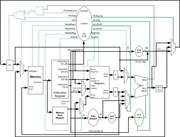
New data Path.
Figure 5.33 .page 383.
##############
1)Instruction fetch step
2)Instruction decode and register fetch
step
3)Execution, memory address computation, or branch
completion
(change the PC with branch target address)
4)Memory access or R type instruction completion
step
5)Memory read completion
step
1)Instruction fetch step
IR =
Memory[PC];
PC = PC
+4;
IR : Instruction
Register.
2)Instruction decode and register fetch
step
A =
GPR[IR[25-21]];
B =
GPR[IR[20-16]];
ALUOUT = PC +4 +
(sign-extend(IR[15-0]) << 2);
3)Execution,memory address computation, or branch
completion
(change the PC with branch target address)
Memory reference:
ALUOut = A +
sign extend(IR[15-0]);
Arithmetic logical instruction(R type)
ALUOut = A op B;
Branch:
if (A = B=) PC = ALUOut;
Jump:
PC = PC[31-28] || (IR[25-0] << 2);
4)Memory access or R type instruction completion
step
Memory reference:
MDR = Memory [ALUOut];
or
Memory [ ALUOut] = B;
Arithmetic logical instruction(R type)
GPR[IR[15-11]] = ALUOut;
5)Memory read completion
step
Load
GPR[IR[15-11]] = MDR;
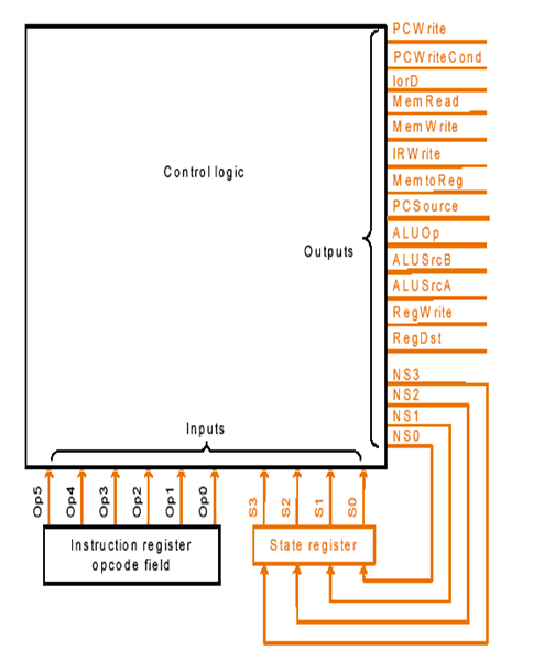
############## Control for Each State
###############
Finite State Machine(FSM).
FSM is used to
specify the multi cycle control.
FSM consists of a set of states and
directions on how to change
states.
FSM
review.
Finite state
machines:
a
set of states and internal storage
next state
function (determined by current state and the input)
output function
(determined by current state and possibly input)
Well use a Moore machine (output based only on current
state)
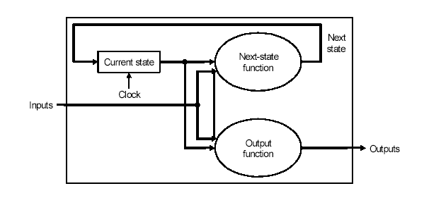
Finite State Machine Concept.
Finite State Machine
Controller
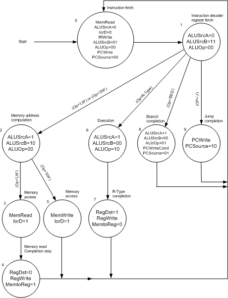
Finite State Diagram Fig. 5.42.
Logic Representative: Logic Equations
· Next state from current
state
· State 0 ->
State1
· State 1 ->
S2,S6,S8,S9
· State 2
->S3,S5
· State 3
->S4
· State 4 ->State
0
· State 5 -> State
0
· State 6 ->
S7
· State 7 -> State
0
· State 8 -> State
0
· State 9 -> State
0
Or How can we reach each
state.
prior state &
condition
S4, S5, S7, S8, S9
-> State0
S0
-> State 1
S1 &(op = sw || op = lw) -> State 2
S2 &op = lw
-> State 3
S3
-> State 4
State 2 & op = sw
-> State 5
S1 & op = Rtype
-> State 6
State 6
-> State 7
S1 & op = beq
-> State 8
State 1 & op = j
-> State 9
Implementation Technique: Programmed Logic
Arrays
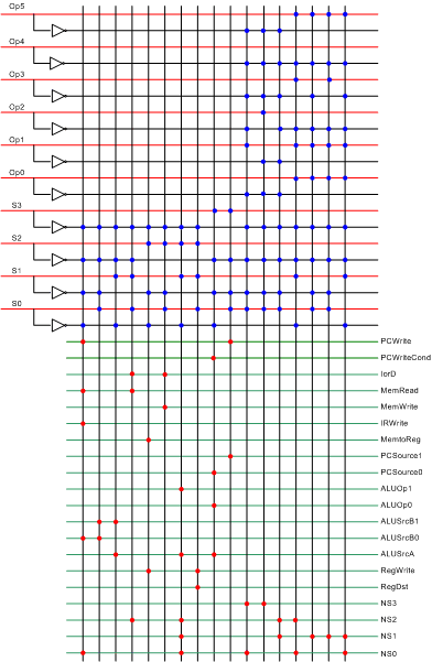
Fig. PLA...
Multi cycle Control
· Given numbers of FSM, can determine
next state as function of inputs,
including current
state
Turn these into Boolean equations for
each bit of the next state lines
Can implement easily using
PLA
What if many more states, many more
conditions?
What if need to add a
state?