EE 4720 1997 Final Exam Solution
|
With a larger-immediate instruction: | |
lw rll, 0(r10)
addli #0x981234
|
Without larger-immediate instructions: | |
lw r11, 0(r10)
lhi r9, 0x98
ori r9, r9, 0x1234
add r11, r11, r9
|
To implement larger-immediate instructions the processor needs
some way of remembering which register was used by the
last arithmetic or logical (ALU) instruction. A last-destination register
in the ID stage would serve: whenever an ALU instruction is
in ID it will write its rd field (the destination register number)
into the last-destination register. When a larger-immediate
instruction is in ID it will use the contents of last-destination
as its destination and rs1 operand register number. | |
|
There is one problem with the solution so far: to retrieve operand
1 ID must first determine that a larger-immediate instruction
is present (otherwise it will use IR bits 6-10 for the register number).
This may lengthen the critical path, so the solution below uses
a register to store the last destination. | |
|
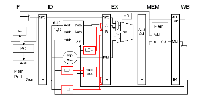
In the solution above, changes are shown in red, and registers have bold outlines.
The "=LI" block examines the instruction opcode and returns 1
if it's a larger immediate, 0 otherwise. The "make xxxi" box
combines a larger-immediate instruction (or control bits)
and the last destination register into a new IR value or control
bits; these are used if a larger-immediate instruction is present.
The new IR value or control bits would be the same as an immediate
type instruction, with the LD contents appearing as rs1 and rd. | |
|
LD is the last-destination register, LDV is the last destination value.
The controller must only clock the LD and LDV registers during
an ALU instruction writeback phase. The sign extension
unit, since it is used for J-type instructions, can already
sign-extend 26-bit quantities.
| |
|
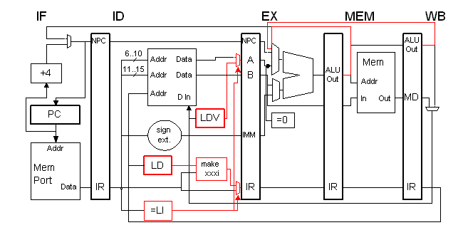
The bypassing changes are minor, connections are added from MEM and WB
back to the ALU. Unlike general-purpose bypass connections, these
only go to the top ALU input.
| |
|
Consider the execution below: | |
Time              0  1  2  3  4  5
add   r1, r2, r3  IF ID EX ME WB
addli #123456        IF ID EX ME WB
|
In cycle 1 the identity of the destination register, r1, is written
to LD. The actual data is written to LDV in cycle 4. The
addli instruction arrives in ID during cycle 2. The makexxxi
box constructs an "addi r1, r1, #123456" instruction, and
the same interlock hardware that detects RAW hazards in
regular instructions (not shown) detects the RAW hazard with the
newly constructed addi, and sets the control bits needed
to use the MEM-to-EX bypass paths (not shown). In cycle 3 the bypass
path is used to connect the new r1 to the top ALU input. | |
|
A simpler solution would place the LDV and LD registers
in the EX stage, avoiding the need for bypass paths. | |
div f0,f10,f11 IF   ID    DV1 DV1 DV1 DV1 DV1 DV1 DV1 DV1 DV1 MF  WBX
mul f0,f3,f2        IF    ID  MU1 MU1 MU2 MU2 MF  WB
add f8,f9,f0              IF  ID              A1  A2  MF  WB
add f0,f1,f2                  IF              ID  A1  A2  MF  WB
mul f3,f0,f4                                  IF  ID      MU1 MU1 MU2 MU2 MF  WB
mul f5,f0,f6                                      IF      ID      MU1 MU1 MU2 MU2 MF  WB
|
Because the initiation interval of the multiply unit is 2, the last
multiply instruction must wait an extra cycle. The problem requires
that "distinct pipeline segments have distinct names", so the multiply
unit's segments are labeled MU1 and MU2. With an initiation interval
of 2, an instruction spends 2 cycles in each segment.
| |
|
Even though its result won't be needed, the divide instruction is
allowed to continue but it will not write the register file (indicated
by a WBX instead of WX.
| |
div f0,f10,f11 IF   ID    7:DV1 7:DV1 7:DV1 7:DV1 7:DV1 7:DV1 7:DV1 7:DV1 7:DV1 7:WB
mul f0,f3,f2        IF    ID    3:MU1 3:MU1 3:MU2 3:MU2 3:WB
add f8,f9,f0              IF    ID    1:RS  1:RS  1:RS  1:RS  1:A1  1:A2  1:WB
add f0,f1,f2                    IF    ID    2:A1  2:A2  2:WB  2:WB
mul f3,f0,f4                          IF    ID    4:RS  4:RS  4:RS  4:MU1 4:MU1 4:MU2 4:MU2 4:WB
mul f5,f0,f6                                IF    ID    ID    3:RS  3:RS  3:RS  3:MU1 3:MU1 3:MU2 3:MU2 3:WB
|
The last multiply spends an extra cycle in ID, waiting for a free multiply reservation
station.
| |
div f0,f10,f11 IF   ID    7:DV1 7:DV1 7:DV1 7:DV1 7:DV1 7:DV1 7:DV1 7:DV1 7:DV1 7:WB
mul f0,f3,f2   IF   ID    3:MU1 3:MU1 3:MU2 3:MU2 3:WB
add f8,f9,f0        IF    ID    1:RS  1:RS  1:RS  1:RS  1:A1  1:A2  1:WB
add f0,f1,f2        IF    ID    2:A1  2:A2  2:WB
mul f3,f0,f4              IF    ID    4:RS  4:RS  4:MU1 4:MU1 4:MU2 4:MU2 4:WB
mul f5,f0,f6              IF    ID    ID                3:RS  3:MU1 3:MU1 3:MU2 3:MU2 3:WB
div f0,f10,f11 IF   ID      DV1   DV1   DV1   DV1   DV1   DV1   DV1   DV1   DV1   WBX
mul f0,f3,f2   IF   ID      MU1   MU1   MU2   MU2   WB
add f8,f9,f0        IF      ID                      A1    A2    WB
add f0,f1,f2        IF      ID                            A1    A2    WB
mul f3,f0,f4                IF                            ID          MU1   MU1   MU2   MU2   WB
mul f5,f0,f6                IF                            ID                      MU1   MU1   MU2   MU2   WB
|
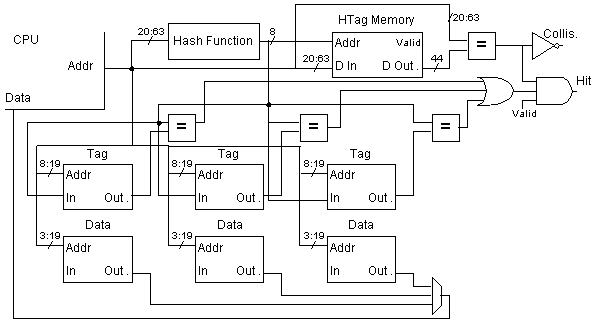
Bit positions: Alignment 0:2, Offset, 3:7; index, 8:19; tag, 20:63.
(In a previous version of this solution bits 0:7 were specified for
the offset. That's okay, as long as all of those bits are not
used to construct an address for the data part of the cache.)
| |
|
Cache size: 3 × 4096 × 256 = 3 & 212×
28 =
3,145,728 bytes. | |
|
To implement include tag, valid, and dirty bit storage:
3 × 4096 (256+(44+1+1)/8)=3,216,384 bytes. | |
double *a = 0x10000000;  /* Assume the entire address space is ours. */

/* Block size is 256 bytes or 32 doubles.  Touch consecutive blocks. */
for( i=0; i<4096; i++ ) total += a[ i * 32 ];

/* To fill set, touch two blocks with different tags than above. */
for( i=0; i<2048; i++ ) total += a[ 0x20000 + i * 32 ] + a[ 0x40000 + i * 32 ];
|
The design is shown in the figure below. The lower part of the illustration
shows a conventional cache, the only difference is that the tag memory
stores 8-bit HTags rather than the 44-bit tags an ordinary cache would use.
The upper half shows the hardware for converting the tag of the accessing
address to an HTag. An HTag memory is provided for storing the full 44-bit
tags corresponding to each HTag, this is needed to detect collisions.
| |
|
(1)When an address with a new tag is presented, the lookup in the HTag
memory will yield an invalid (perhaps never written) HTag. The new
tag will be written to the HTag memory. This could only be a cache miss;
the remainder of the accesses proceeds as a normal miss.
| |
|
(2) If an address is presented with an already cached tag the
value retrieved from the HTag memory will be valid and will
match the tag of the access address.
| |
|
(3) When an address collides with a tag the value retrieved from
the HTag memory will not match the access address. This means
that two different addresses have the same HTag (a risk when
squishing 44 bits to 8), one of these is for cached item(s)
the other is the current access. This is trouble because those
already cached items have to be evicted before the current
access can be cached. (Otherwise there would be no way to
distinguish them.) The lines to be evicted could be anywhere,
so eviction will be time-consuming, perhaps performed by software
(using a trap routine).
| |
|
Not shown is the control input to the data multiplexor. That
would be derived from the three HTag comparison boxes (which
connect to the or gage). The valid input to the and gate
also comes from the tag memories. Note that the collision signal is
meaningless when the valid output of the HTag memory is false.
| |
|
The data to write will not be ready until the end of a
cycle and will be needed at the beginning of the next cycle. With
many inputs and outputs, it can take longer for a signal to reach
its destination on a CDB than on a bypass path, which has
fewer inputs and outputs. | |
|
A benchmark suite is more appropriate for overall
performance evaluation, the engineers might use it to assess the net
effect of many changes. Synthetic benchmarks might be designed to
test and tune specific hardware features. The engineers might use it
to determine why a particular branch prediction scheme is or is not
effective.
| |
Time 0   1   2   3   4   5
lw   IF  ID  EX  MEM WB!
sub      IF  ID  EX  MEM EX
add          IF  ID! EX! MEM
mul              IF  ID  EX
sw

<trap>               IF  ID
|
The pipeline checks for exceptions in the WB stage. The
add exception at cycle 2 results in add being nulled and
an exception code being passed along with the nulled instruction. (The
exclamation point indicates the instruction is in that stage and is
nulled because of an exception.) Suppose memory access done by the
lw instruction results in a page fault; this would occur
at cycle 3, and would result in a trap being inserted--for the
lw instruction--in cycle 4, replacing the
sw that was being fetched. | |
|
It's similar since dependencies must span several instructions so
that multiple instructions can be issued in parallel. With
superscalar processors that scheduling is optional, unscheduled code
would run but with more stalls. VLIW describes an ISA (although an
implementation is often what's meant) so code in non-VLIW ISAs must be
recompiled. Unlike superscalar processors, VLIW sub-instructions
issued in parallel cannot have any dependencies (in correct code). | |
|
As m increases prediction accuracy improves as a
branch's global-history-dependent behaviors can be individually maintained.
As m increases further, two effects can reduce performance. First,
a greater number of branches might share the same entry. Second,
a greater amount of irrelevant global history might spread a
branches counters thin. With 10 bits of correlation (m=10),
each branch would have 1024 counters, if the least recent five branches
were irrelevant and evenly distributed, then each useful behavior
would have to be "learned" by 32 counters. | |


