| Problem 3 (c), EE 4720 1997 Final Exam Solution | Top |
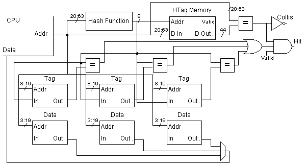
| The design is shown in the figure below. The lower part of the illustration shows a conventional cache, the only difference is that the tag memory stores 8-bit HTags rather than the 44-bit tags an ordinary cache would use. The upper half shows the hardware for converting the tag of the accessing address to an HTag. An HTag memory is provided for storing the full 44-bit tags corresponding to each HTag, this is needed to detect collisions. |
| (1)When an address with a new tag is presented, the lookup in the HTag memory will yield an invalid (perhaps never written) HTag. The new tag will be written to the HTag memory. This could only be a cache miss; the remainder of the accesses proceeds as a normal miss. |
| (2) If an address is presented with an already cached tag the value retrieved from the HTag memory will be valid and will match the tag of the access address. |
| (3) When an address collides with a tag the value retrieved from the HTag memory will not match the access address. This means that two different addresses have the same HTag (a risk when squishing 44 bits to 8), one of these is for cached item(s) the other is the current access. This is trouble because those already cached items have to be evicted before the current access can be cached. (Otherwise there would be no way to distinguish them.) The lines to be evicted could be anywhere, so eviction will be time-consuming, perhaps performed by software (using a trap routine). |
| Not shown is the control input to the data multiplexor. That would be derived from the three HTag comparison boxes (which connect to the or gage). The valid input to the and gate also comes from the tag memories. Note that the collision signal is meaningless when the valid output of the HTag memory is false. |
| David M. Koppelman - koppel@ee.lsu.edu | Modified 8 May 1998 18:54 (23:54 UTC) |